Industry
 Num:26
 See:17885
2020-09
22
MOS tube output characteristic curve, do you understand?
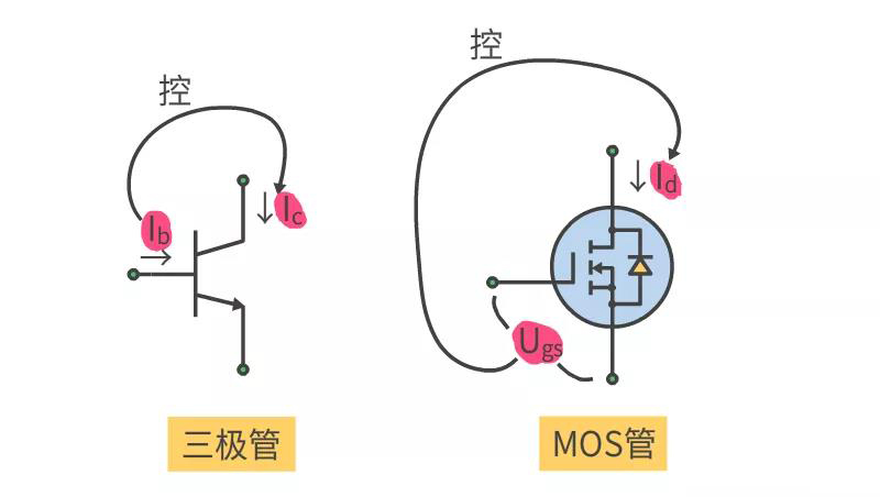
We know that the transistor USES the ID current to control the current IC so the transistor is the current control current device.

The MOS tube USES the voltage of VGS to control the current ID, so the MOS tube is a voltage control current device.
For N channel enhanced MOS tube, when VGS>VGS(th), MOS will start to conduct. If a certain voltage is added between D and S poles, a current ID will be generated.
Under a certain VDS, the current Id of D pole is related to the voltage VGS of G pole.
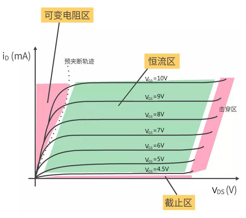
First, let's take a look at the output characteristic curve of MOS tube. The output characteristic of MOS tube can be divided into three areas: cut-off area, constant current area and variable resistance area.

MOSFET output characteristic curve
Cut-off region: When VGSThe cut-off region is near the abscissa at the bottom of the output characteristic, indicating that the MOS tube cannot conduct electricity and is in the cut-off state. Cut-off zone is also called clipping zone, in which all channels are clipped, the current Id is 0, and the pipe does not work.
Constant current region: When VGS≥VGS(th) and VDS≥ VGS-Vgs (th) are met, THE MOS tube enters the constant current region.
The constant current region is in the middle of the output characteristic curve, and the current ID basically does not change with VDS. The size of THE Id is mainly determined by the voltage VGS, so it is called the constant current region, also called the saturation region. When MOS is used for amplification circuit, it works in the constant current region (saturation region).
Note: The constant current region (saturation region) of MOS tube output characteristics is equivalent to the amplifier region of triode.
Variable resistance area: when VGS>VGS(th) is met and VDS< VGS-VGS (th) is met, MOS tube enters the variable resistance area.
The variable resistance area is at the left of the output characteristic, and Id increases with the increase of VDS. The two are basically linear, so they can be regarded as a linear resistance. When VGS is different, the resistance value will be different, so in this area, the MOS tube is a variable resistance controlled by VGS.
The breakdown area is on the left side of the output characteristic. With the increase of VDS, the PN junction suffers too much reverse voltage and is broken down. The pipe should be avoided to work in this area.
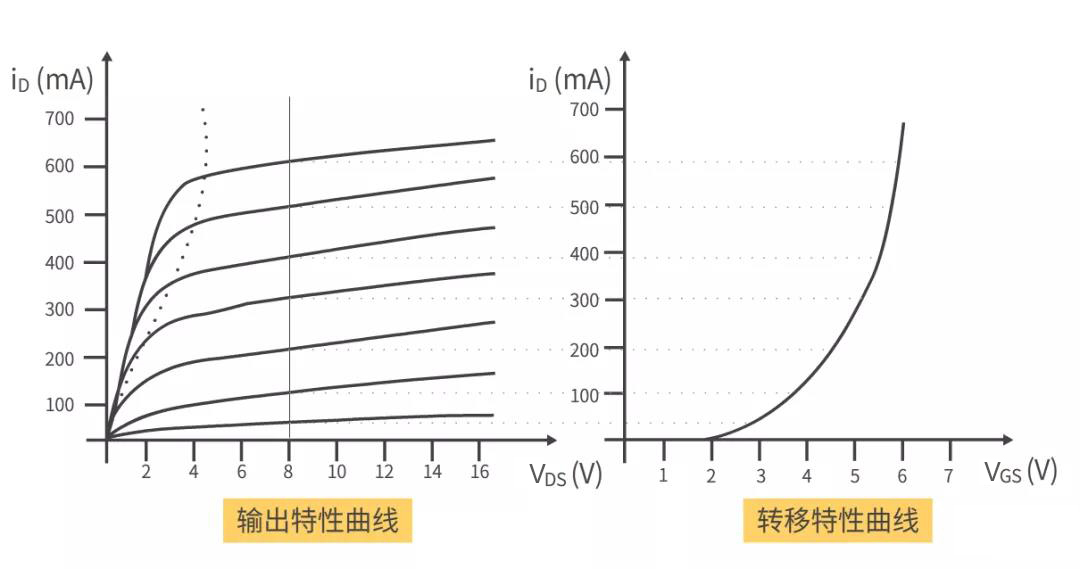
According to the output characteristic curve of MOS tube, for example, take the point VDS=10V as shown in the figure below, and then use the method of drawing to obtain the corresponding transfer characteristic curve.

The transition property is the relationship between Id and VGS when VDS is constant.
In the transfer characteristic curve in the figure above, we can see that when VGS is greater than 4V, Id increases greatly, while when VGS is greater than 5V, Id basically does not change greatly.
In the transfer characteristic curve in the figure above, we can see that when VGS is greater than 4V, Id increases greatly, while when VGS is greater than 5V, Id basically does not change greatly.

Share


站LOGO.png)


.jpg)